Imperfect crystal structure models
dislocations, defects and epitaxial growth
Crystal structure models are perfect for illustrating crystal structures but, in reality, few crystals are themselves perfect. Real crystals are subject to the laws of thermodynamics, and the influence of entropy prevents the existence of perfect crystalline order.
Dislocations
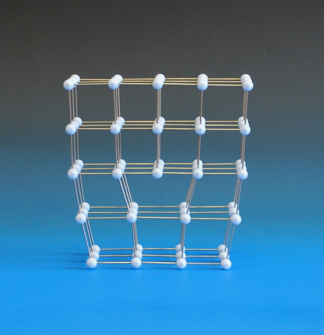
There are actually relatively few ways in which dislocations can form in crystals, and we are able to model any of them. The most commonly encountered are the screw dislocation and the edge dislocation. Our screw dislocation model has proved difficult to satisfactorily image, but the image below is adequate:
Edge dislocations are more readily understood when depicted within a primitive cubic lattice but, if you require it, we can create the dislocation within other lattices, such as the body centred cubic lattice shown (left).
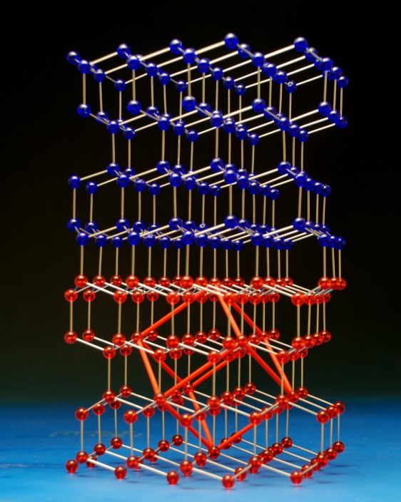
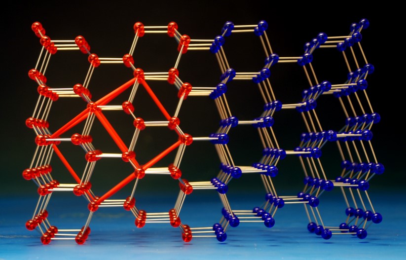
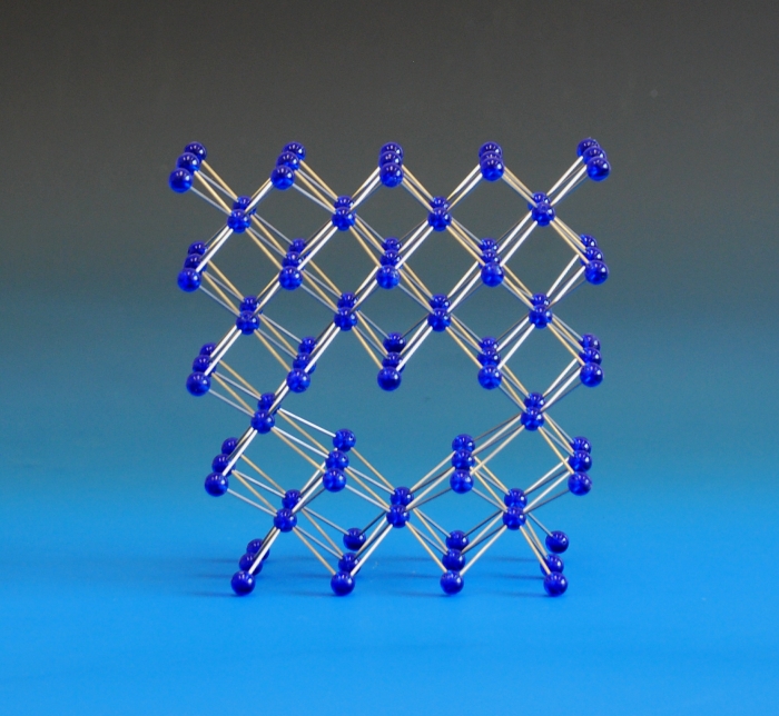
Other common dislocations include the 60° dislocation in the diamond structure, where two adjacent layers in the 110 direction are rotated by 60° (or, equivalently, 180°) with respect to each other:
Crystal structure model of Silicon with the unit cell highlighted a 60° dislocation between the red and blue regions. A highlighted unit cell is included in the model.
This dislocation is just one example of a stacking fault - more complex stacking faults inevitably lead to much larger models, and while it is only rarely that we are asked for such models, we can make up any stacking fault you want. Twin boundaries and antiphase boundaries are relatively straightforward; grain boundaries - large scale dislocations between grains that sit at an angle to one another are probably more complex to make up than almost any other model that we make.
Epitaxial growth
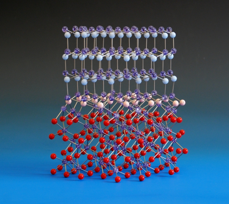
Models of epitaxial growth are closely related to those of dislocations, in that two layers in a structure are mismatched - the only real difference being that the two layers comprise different materials. The most appropriate materials for epitaxial growth tend to have closely matched unit cell parameters, such as in the epitaxial growth of GaN on Al2O3.
Epitaxial growth of GaN on Alumina.
Point defects
Point defects are relatively easy to introduce into models, so the depiction of vacancy defects and interstitial defects, such as Frenkel pairs or Schottky defects, , substitutional defects, or antisite defects can be incorporated into just about any appropriate model with almost no additional costs.

